
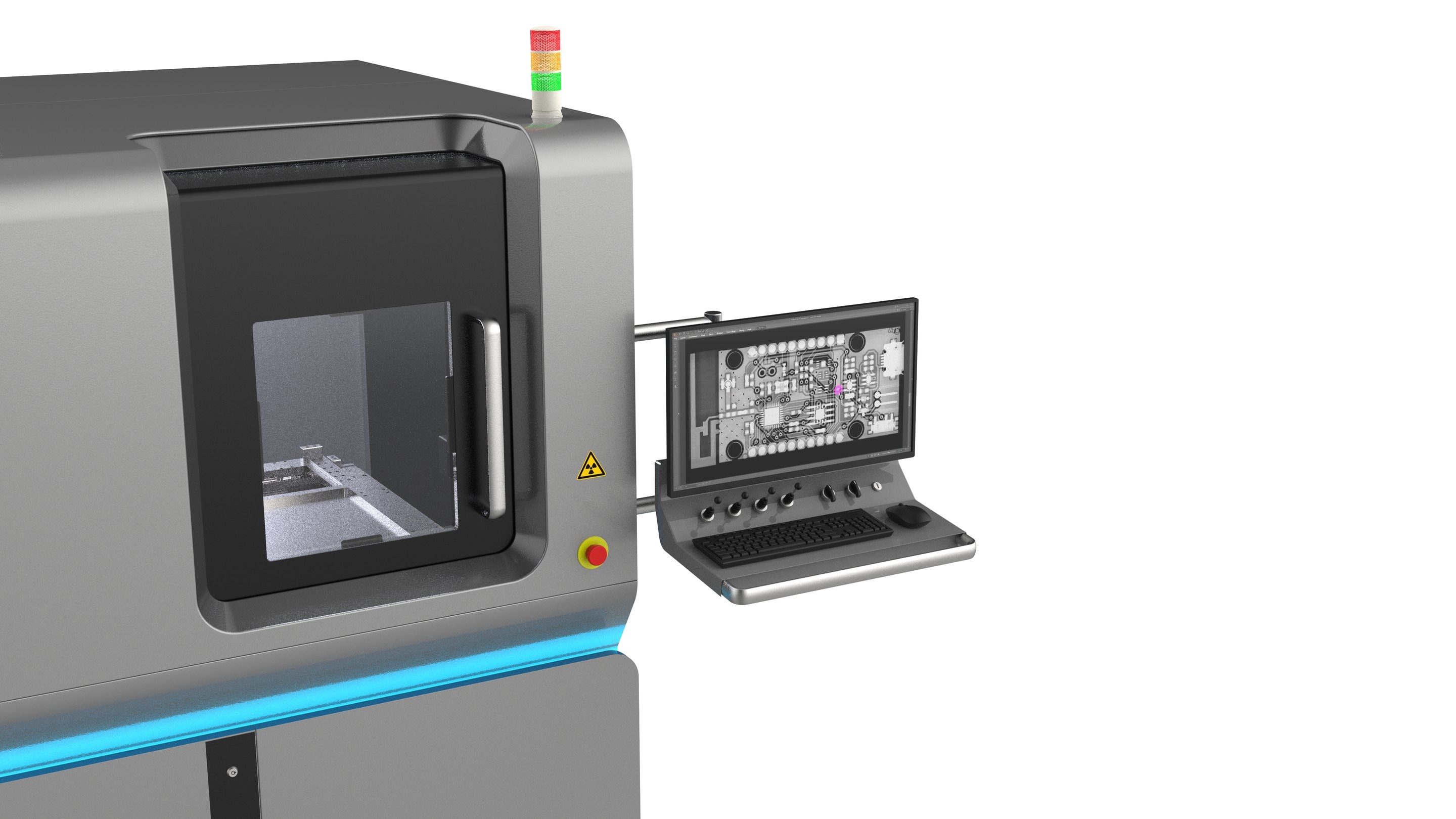
MQX.tracE · 2.5D X-ray for electronics
Engineered to reveal the invisible.
India's first indigenous 2.5D PCB X-ray inspection system, built for micron-level defect detection in high-density electronic assemblies, revealing solder voids, cracks, bridging, missing BGAs and PTH fill issues that visual inspection cannot catch.
One platform. Three depths of answer.
Where 2D leaves ambiguity, MQX.tracE CT adds 3D slicing and reconstruction to isolate layers, verify internal geometry and generate evidence-ready reports without destructive sectioning. MQX.tracE | IN-3D brings inline 2D / 2.5D / 3D inspection and automated defect analysis directly into the production line. All three systems share an AI-powered imaging suite.
MQX.tracE · 2.5D
Micron-level defect detection for electronics.
Micron-level defect detection
For BGAs, QFNs, QFPs and PTH solder joints, defects measured in microns rather than millimetres.
AI-powered software
Standardized inspection and faster reporting, with less operator subjectivity.
High-throughput ready
Macros and batch inspection to scan boards in sequence.
Large inspection coverage
Very high magnification across dense assemblies.
AERB-certified safety
Leakage radiation below 1 µSv/hr for operator-safe use.
System features at a glance.
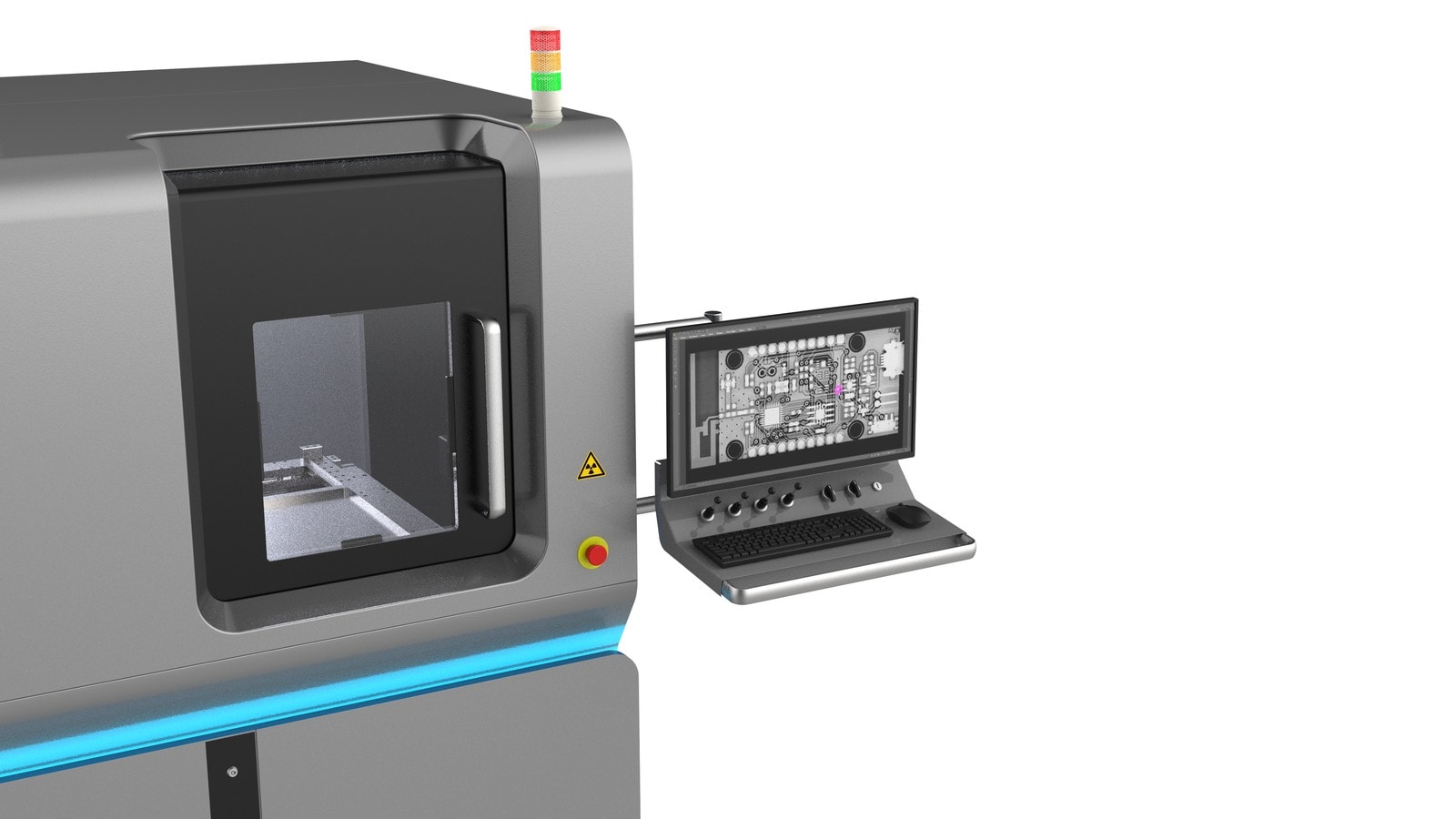
MQX.tracE CT
2D gives answers. CT gives certainty.
For complex electronics, 2D views can be ambiguous because layers overlap. MQX.tracE CT combines high-clarity 2D screening with 3D slicing and reconstruction, so teams can isolate layers, verify internal geometry, confirm root cause and generate evidence-ready reports, without cutting a board apart.
Layer-by-layer CT visibility
Separate overlapping features and reduce escapes.
Faster failure analysis and R&D cycles
Evidence-ready slices with no physical sectioning.
Standardized inspection workflows
Manual, semi-automatic and automatic modes, plus macros.
Advanced measurement tools
Package and semiconductor analysis with pass/fail support.
Safe, compliant operation
Radiation safety below 1 µSv/hr at the cabinet surface.
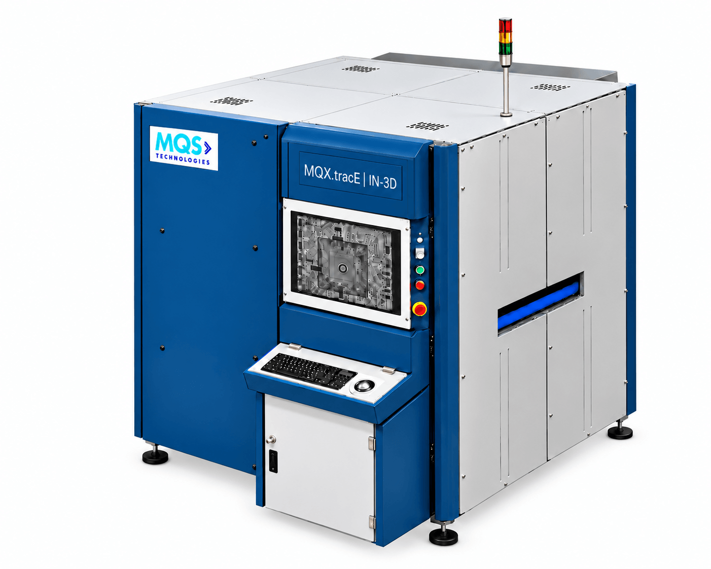
MQX.tracE | IN-3D
Inspection built into the SMT production flow.
An inline X-ray solution for PCB and electronic assemblies, combining 2D / 2.5D / 3D inspection, automated defect analysis, in-line board handling and Industry 4.0 integration without moving boards to an offline station.
Inline multimode inspection
Run routine 2D screening, oblique 2.5D inspection and full 3D analysis on one production-line platform.
Automated defect analysis
Standardize defect detection and retain inspection results and per-joint measurements for production traceability.
Production-line board handling
A linear motor and pneumatic clamping move boards through inspection without transferring them to an offline station.
Industry 4.0 integration
Write inspection results back to ERP and SPC systems for closed-loop quality monitoring.
Sample inspection images.
Representative captures from MQX.tracE, MQX.tracE CT and MQX.tracE | IN-3D.
Technical Specifications
Three systems, quoted separately. For 2.5D and CT, JIMA resolution describes the smallest feature the system can resolve. IN-3D detector resolution is stated as pixel pitch.
MQX.tracE · 2.5D
- X-ray energy range
- 20 – 160 kV
- Max target power
- 25 W
- Tube type
- Microfocus, open type, transmission target
- JIMA resolution
- 0.9 µm
- Detector active area
- 161 × 161 mm
- Pixel pitch / frame rate
- 105 µm / 40 fps
- Manipulator
- 6-axis, servo motors with encoder
- Magnification
- Geometric above 1,900×; system above 7,000×
- Radiation safety
- AERB type-approved; leakage below 1 µSv/hr
- Footprint / weight
- 2200 (H) × 1800 (W) × 1900 (D) mm; approx. 4500 kg
MQX.tracE CT
- Power
- AC mains 220 – 230 V, 50 Hz, single phase
- Anode voltage
- 30 – 160 kV
- Target power
- Up to 15 W
- X-ray source
- Open tube, transmission target
- Resolution
- 0.75 µm or better
- Magnification
- Geometric up to 3,000×; total up to 7,500×
- Imaging
- Above 1 MP; 10 fps; 16-bit ADC
- Manipulator
- Five-axis; 360° rotation, ±70° tilt
- PCB capacity
- Max 440 × 550 mm; inspection area 310 × 310 mm; sample weight 5 kg
- Inspection modes
- Manual / semi-automatic / automatic, plus macros
- CT capability
- 3D CT slicing and reconstruction
- Radiation safety
- Below 1 µSv/hr at cabinet surface
- Image export
- RAW / JPEG / TIFF / GIF / BMP
- Vibration mitigation
- Anti-vibration supports for stability
MQX.tracE | IN-3D
- X-ray source
- Sealed microfocus source, 130 kV, 39 W, 11 µm focal spot
- Detector
- High-resolution flat panel detector, 105 µm pixel pitch, 16-bit depth, 40 fps, real-time acquisition
- Imaging modes
- 2D / 2.5D / 3D
- PCB capacity
- Minimum 50 × 50 mm; maximum 610 × 510 mm
- PCB thickness
- 0.4 – 6 mm
- Maximum board weight
- 5 – 8 kg
- Board handling
- Linear motor with pneumatic clamping
- Dimensions with conveyor
- 3000 × 2186 × 1860 mm
- Dimensions without conveyor
- 1600 × 2186 × 1860 mm
- System weight
- 2500 kg
- Software
- MQS Imaging Suite on Windows, with acquisition, review and manipulator control
- Production integration
- Results and per-joint measurements written back to ERP and SPC
Compare all three on your own boards
Request a demonstration of MQX.tracE 2.5D, MQX.tracE CT and MQX.tracE | IN-3D against your inspection requirement.